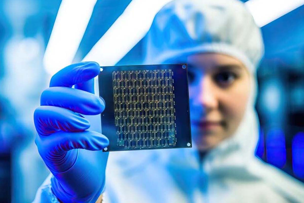
Wafer Probe Testing
Wafer testing has long been used to evaluate bare dies that are still part of the wafer. This process allows for testing the wafer in its native form and separating good dies that require further testing from those that fail initial testing. Traditionally, the testing process is divided into steps, including “Wafer Test,” “Wafer Probe,” or “Probe,” and the Final Test, which involves testing parts after they are packaged. The Final Test may include multiple stages, such as structural insertion, SerDes loopback testing, post burn-in testing, and hot or cold insertions.
Even in wafer testing, temperature-based testing can be performed, known as the “Hot Chuck Test” or “Cold Chuck Test.” Here, “chuck” refers to the base on which the wafer rests, as shown in Fig. 1. The probe system, which includes the thermal control system and the probe card, is illustrated in Fig. 2.

Figure 1. A Wafer prober Chuck (MPI corporation)

Figure 2. A Wafer Probe system (Seica.com Wafer probe card)
The cost of the probe card is influenced by several factors: the density of the probe needles, which depends on the pad pitch, the current-carrying capacity of the probe needles, and the number of signal and power probe pins required by the design. The speed at which the probe pin can transmit data is determined by the probe card design and the parasitics of the probe circuit. Typically, probe systems have high parasitic elements, which impose additional restrictions on the probe test patterns.
As packaging costs increased, the need for more comprehensive wafer probe screening grew, aiming to prevent defective parts from being packaged. When parts began to be packaged in different formats based on partial core functionality, wafer testing became essential to bin dies according to their partial cores. Parts tested for defects during the wafer probe stage were further tested after packaging to identify additional defects. Depending on the test flow, different tests—such as temperature binning and external loopback for SERDES—were performed at various Final Test (FT) stages.
A critical test for device reliability was the 40-hour burn-in, where devices were placed in burn-in ovens and subjected to burn-in patterns (toggle patterns) at elevated temperatures and voltages to eliminate early failures. Typically, burn-in was performed on packaged parts in burn-in ovens, followed by testing to remove the failed parts.
Known-good-Die KGD
As probe technology advanced, the need arose to test devices thoroughly at the wafer level and produce defect-free devices, including reliability screening. This led to the implementation of wafer burn-in to ensure the quality required by customers. Manufacturers could then procure these known-good-dies (KGD), package them, conduct a final QC test, and ship the parts to customers. This approach made volume production more efficient and streamlined, optimizing the total cost of the final product. KGD binning for monolithic chips is particularly used for high-volume, cost-sensitive parts.
As we progress to 2.5D and 3D packaging, it has become crucial that all dies assembled in the final package are KGDs, ensuring that the final System-in-Package (SiP) is not discarded due to a defective part. The high cost of assembling these packages makes discarding them due to defective dies prohibitively expensive, potentially driving up the final product cost to uncompetitive levels. Therefore, the need for KGDs in 2.5D and 3D devices is paramount.
Building KGDs for 2.5D and 3D systems introduces several additional challenges. The first challenge is that most of these devices are assembled using silicon or glass interposers, which require dies to have through-silicon vias (TSVs) connecting to the silicon wafer’s backside. This necessitates thinning the KGD to 10 micrometers, which can introduce thermal and mechanical issues. It may also require testing the part in its thinned form to ensure it remains a known good die when assembled.
The second challenge is that as we design systems with KGDs and interposers, we can interconnect the dies through the interposers using pads with a pitch of less than 40 micrometers. This density allows for very wide buses with low power consumption per bit per GHz to interconnect the dies. However, this requires careful attention to testing, debugging, and providing redundancy for these buses.
Finally, additional structures must be included on these KGDs to facilitate testing after packaging, ensuring that the final assembled System-in-Package (SiP) is defect-free.
As geometries shrink and the ability to add more transistors per unit area grows, Moore’s Law has encountered challenges at smaller scales. At sub-10nm geometries, defect density poses significant challenges to achieving defect-free devices. In older process technologies above 10nm, system designers aimed to place as many transistors on a single monolithic silicon die as possible, limited by the Reticle limit—the largest mask size that can be built. Large dies, however, face yield losses due to defect density, which has prompted silicon and system designers to reconsider the economics of die sizes in semiconductor manufacturing.
One solution has been the adoption of 2.5D or 3D silicon chips, where dies are interconnected using Through-Silicon-Via (TSV) technology, either in a planar arrangement or a vertical stack. In the planar arrangement, these dies are connected via a silicon interposer, which is made from an older technology, leading to better yields. Two silicon interposer-based technologies are commonly used: Chip-on-Wafer-on-Substrate (CoWoS) from TSMC and Embedded-Multidie-Interconnect-Bridge (EMIB) from Intel. Both methods require die thinning for TSVs. As technology progresses, glass interposers have been proposed as an alternative to silicon interposers, offering better parasitic control and improved manufacturing characteristics.
One reason system designers prefer to avoid sending data off-chip is that when signals are sent off-chip, they must travel longer distances, increasing resistance and capacitance. This requires boosting the drive strength, which slows down signal speed and increases power consumption. Additionally, on a package and PCB, the distance between pad bumps must be large to accommodate bump wires and align with PCB feature sizes. This increases the I/O pad pitch, reducing the density of wires that transmit and receive signals from the chip. Various techniques have been developed to address these issues, such as double data rate (DDR) I/O, which transmits data on both edges of the clock, and SERDES, which serializes data to reduce the width of wide bus transmissions. Differential signaling with lower voltage swings is used to increase transmission speed.
While these advancements allow for high-speed data transmission, they consume considerable power and, in some cases, introduce signal latency, which must be compensated for in system design. Silicon interposers offer a solution by providing higher I/O density for die-to-die connections, achieving distances as short as 10 micrometers compared to the 130-micrometer pitch of package pad interconnects. Because all connections are made on silicon, the shorter interconnects and lower parasitics enable higher-speed signals at lower drive strengths, reducing power consumption in off-chip interconnects.
Your text provides a clear description of the evolving interconnect technologies and testing strategies for Known Good Dies (KGDs) in advanced 2.5D and 3D packaging. Here’s a slightly refined version for clarity and flow:
With the ability to build wider off-die interconnect buses at lower power, new interconnect technologies have emerged. One of the most popular is High Bandwidth Memory (HBM), which offers a very wide memory interface between the logic die and the memory die. HBM is also a 3D-stacked die, combining multiple DRAM dies to significantly increase DRAM bit density while enabling higher bandwidth access with lower power consumption.
For logic-to-logic die interconnects, several new standard bus interfaces have been developed, including the Universal Chip Interconnect Express (UCIe) and the Bunch of Wires (BOW) standards. The current KGDs we are focusing on, which will be used in 2.5D and 3D packaging, will feature Through-Silicon Vias (TSVs) either within the die itself or connected to a TSV-based interposer.
Additionally, these dies are expected to have wide, high-speed interfaces based on standard die-to-die interface bus standards. The test and Design-for-Test (DFT) developments for these KGD dies will incorporate strategies for bare die testing in a wafer probe environment. Moreover, these dies will have a much denser pad pitch for die-to-die interconnects, necessitating advanced testing methods to address these new interconnects.
Known Good Die in 2.5D and 3D silicon
Over the years, there have been significant advancements in KGD and probe testing. Developing probers for advanced devices with increasingly smaller pad pitches has been a key focus. Managing increased active power supplies with better transient responses is also a critical factor. Additionally, KGD requirements often necessitate more comprehensive temperature corner testing, which is a crucial development aspect. Ensuring the reliability of devices for mission-critical applications involves addressing infant mortality through wafer burn-in processes.
A critical aspect of delivering KGDs for current systems is the planning and implementation of Design-for-Test (DFT) strategies that move much of the required instrumentation onto the silicon. As current designs demand higher power and better transient response, it is essential to ensure effective test planning to manage power while keeping test times within acceptable limits. Traditionally, wafer testing focused on yield-limiting tests and redundancy repairs at the probe stage to significantly reduce packaging failures. More complex tests, such as device trimming, loopbacks, and burn-in, were typically postponed to the Final Test phase.
With KGDs, however, all defect screening tests must be performed at the probe stage. This transition requires careful DFT planning to manage test time, test data volume, and test power effectively.

Figure 3. 2.5D packaged SiP
DFT for KGD
Testing large silicon dies at the probe stage requires extensive Design-for-Test (DFT) to minimize test costs and manage data volume effectively. Since probe testing cannot utilize active cooling, thermal considerations dictate that tests be conducted at lower power levels, often below the functional power requirements that would include active cooling.
As the number of package pins increases, the cost of the probe card rises significantly. This necessitates a reduction in the number of active logic pins required for testing, leading to the use of reduced pin test methods. Additionally, the power supplied by each Vdd port is limited. To manage costs associated with a large number of pads, only the power pads necessary for the test’s power profile are utilized.
Balancing test power, probe card cost, test time, needle replacement concerns, and overall test quality is crucial to meeting KGD objectives. This requires careful analysis and optimization to ensure that the test setup aligns with both cost constraints and performance goals.
SERDES Test and loopbacks
For today’s complex System-on-Chip (SoC) designs, there are often numerous SERDES I/Os. Testing these SERDES typically involves near-end and pad loopback tests, allowing for a loopback between the Tx and Rx ports of the SERDES. For die-to-die interconnects, which are usually high-density, redundancy may be incorporated to facilitate repairs and recover functionality in some dies.
SERDES impedance trimming can be performed at the package level. To support this, updates to the One-Time Programmable (OTP) or eFuse settings should be enabled both at the probe stage and during the Final Test (FT).
Memory BIST and Repair
Modern SoCs often include a large number and a diverse range of memory types. As memory density increases, die recovery and repair strategies are extended to accommodate both large and small memories. To conserve fuse bits, a fuse register for smaller memories is assigned to a cluster of small memories, under the assumption that only one memory in the cluster will need repair. Each memory typically includes redundant rows or columns, but the expectation is that only one memory in the entire set will fail. Therefore, Built-In Redundancy Analysis (BIRA) and Built-In Self-Repair (BISR) are performed on the entire cluster, with possible repairs executed at the cluster level.
For larger memories, comprehensive testing is required, including retention tests, weak bit tests, and pattern-sensitive fault tests. Due to variations and pattern sensitivity, background patterns and addressing faults should be tested thoroughly. Some of these tests require applying very low voltages to the memory cells, necessitating isolated and accessible VDDM and VSSM pads connected to the probe card.
Incremental repairs should be enabled for memories to allow for repairs during Final Test (FT), even if repairs were performed during probe testing. This is important because different voltage corners (VT) may need to be exercised under varying conditions post-packaging. Incremental repairs can improve the likelihood of retaining the die and thus enhance the yield of the System-in-Package (SiP) after packaging.
Logic and Scan Testing
Hierarchical design involving multiple place-and-route (P&R) blocks necessitates a hierarchical Automated Test Pattern Generation (ATPG) approach. Each P&R block should include test controllers that can be configured directly at the IP or block level. These blocks need to be wrapped with either shared or dedicated wrappers, with various modes and constraints applied using Test Data Registers (TDR). Further details on test controllers for KGD and integrated packaged systems will be discussed later.
A key aspect of hierarchical ATPG is that IP blocks should have their own test controllers and compression engines. It is preferable to use a Streaming Scan Network (SSN), which allows for the independent development of scan infrastructure for each block, optimizing shift speed and scan chain length according to the block’s requirements. Additionally, implementing low-power scan modes is recommended, as ATPG testing at both probe and package stages may be sensitive to the overall power consumption of the Device Under Test (DUT) configuration.
Given the sensitivity of test time at the probe stage and the need to meet KGD quality goals, test coverage and defect coverage are critical. This may require adding test points to either improve coverage or reduce vector count, or both. To address outliers, the design may need to be validated over a wider range of operating conditions. Incorporating additional fault model patterns, such as IDDQ, small delay patterns, and cell-aware patterns, will enhance defect coverage and improve the quality of Known-Good-Die.
System Level Test
As designs become more complex and process technologies advance, structural testing alone may not cover all conditions that could lead to defective devices. To improve coverage and ensure a working Known-Good-Die (KGD), functional testing of the device may be necessary.
During probe testing, running functional diagnostics without system resources requires loading diagnostics into system caches. This involves executing the diagnostics, enabling internal monitors to enhance coverage, and collecting failure signatures. The process typically involves loading the diagnostics into the cache, running them, and then allowing the results to be scanned out.
To achieve this, modes that support high-speed interfaces for loading and reading from caches can be employed. These interfaces can also be used to load structural patterns at speed, facilitating efficient functional testing and improving overall test coverage.
On Test Controllers
When using Known-Good-Die (KGD) in a multi-die stack, it is important to consider that the bare die controllers located at the edge of the device will be integrated into the multi-die configuration. At the multi-die integrated level, it will be necessary to port patterns from the edge of the KGD to the top level of the System-in-Package (SiP). This process includes transferring both the patterns and the Pattern Description Languages (PDLs).
To facilitate this, standalone test access points (TAPs) on the KGD need to be converted into embedded TAPs (eTAPs) for cleanly porting PDLs and patterns from lower-level KGDs to the top level. Extending Streaming Scan Data (SSD) from the lower-level KGD to the SiP top can streamline this process by enabling pattern retargeting through the SSD infrastructure.
An optimal approach would be to implement an IEEE 1687-based Infrastructure Component Layer (ICL) network in the KGD and convert the 1149.1 top TAP into an eTAP upon integration into the top TAP. Alternatively, IEEE 1838 infrastructure could be used to interconnect die test controllers.
Additionally, mechanisms must be developed to access the scan data on the Known-Good-Die in the packaged SiP. The preference is to access the Streaming Scan Network if it is present on the Known-Good-Die. This may require these I/O for the KGD to drive larger loads on the package part.


